Table Of Content
Printed circuit boards have become incredibly popular over the years due to their many advantages over other types of wiring and connection methods. One of the main reasons for their popularity is their cost-effectiveness. PCBs can be mass-produced using automated processes, which reduces the manufacturing cost and makes them a more affordable option for electronic manufacturers. A printed circuit board (PCB) is a board made of insulating material with a thin layer of conductive material, typically copper, laminated onto its surface. The traces are designed to provide the correct voltage and current levels to each component while minimizing interference and ensuring reliable operation.Components are mounted to the board in order to form useful circuits. The components mounted on a PCB can include resistors, capacitors, diodes, transistors, and integrated circuits, among others.
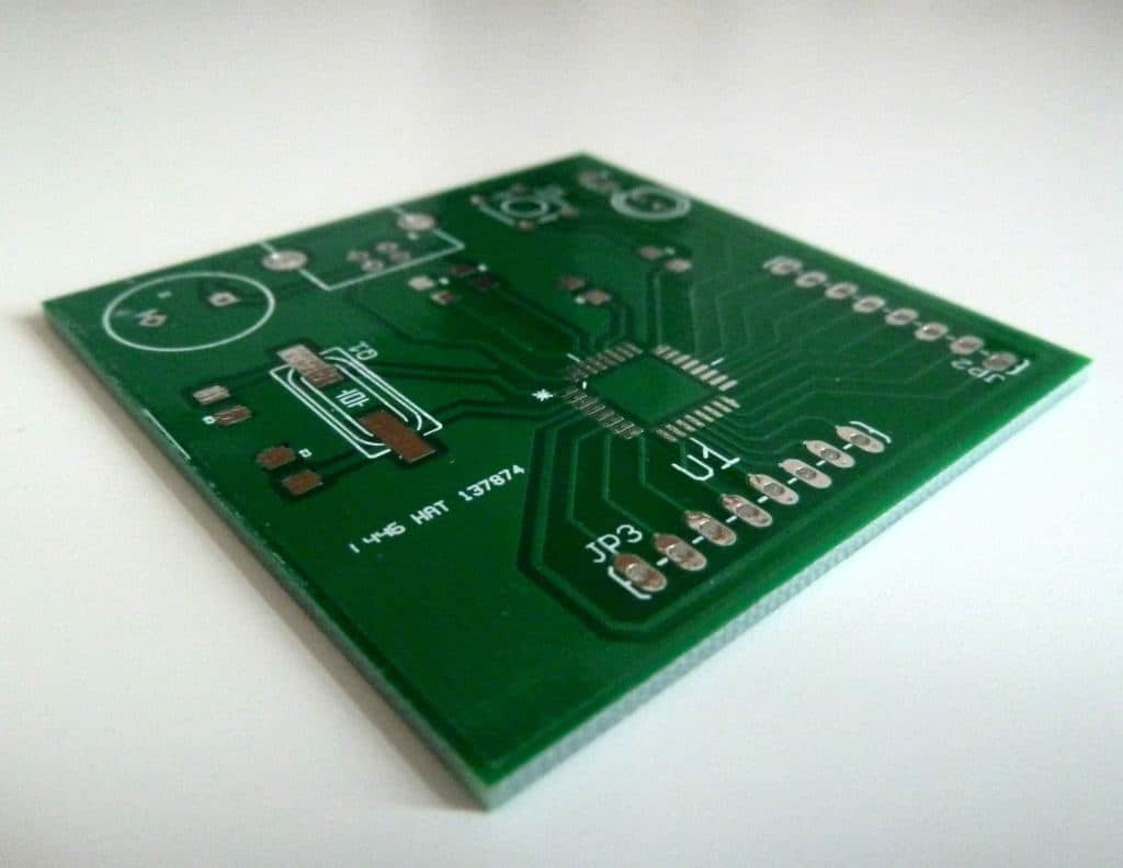
The Composition of a PCB — Printed Circuit Board Components
Once you’ve determined your device requirements for your application, Altium Designer allows you to encode these specifications in design rules. You can rest assured your layout will comply with your design rules, and you can check and correct any rules violations quickly and easily. These rule definition and checking features help you stay within standard design guidelines and help you build a device that meets your technical requirements.
10 practical tips for designing custom PCB art « Adafruit Industries – Makers, hackers, artists, designers and engineers! - Adafruit Blog
10 practical tips for designing custom PCB art « Adafruit Industries – Makers, hackers, artists, designers and engineers!.
Posted: Mon, 08 Apr 2024 07:00:00 GMT [source]
DigiKey Factory Tomorrow Season 3: Sustainable Manufacturing
You’ll want to keep these components away from other parts that are heat sensitive, such as thermocouples and electrolytic capacitors. If those capacitors get too hot, they’ll start to lose their ability to retain a charge. Finally, you need to check everything in regards to your design on completion, before working with the right manufacturer. This is to ensure you haven’t missed anything; if you don’t check beforehand and something is wrong, you’ll have to go through the creation process all over again.
Section 4 – PCB Design: Component Placement
Heat sinks are metal structures that are attached to high-power components to provide a large surface area for heat dissipation. By conducting heat away from the component and into the surrounding air, heat sinks help to reduce the component's operating temperature and prevent overheating. Thermal vias and heat sinks are two commonly used techniques for dissipating heat from a PCB and its components. Thermal vias are small, plated holes that are strategically placed in the PCB to provide a low-resistance thermal path from the component to the PCB's exterior.
Printed Circuit Board (PCB) design is a crucial aspect of modern electronics, serving as the foundation for the development and manufacturing of electronic devices. PCBs are the backbone of electronic products, providing the necessary interconnections and support for various components. The PCB design process involves creating a layout that optimizes the placement of components, routing of traces, and ensuring the overall functionality and reliability of the circuit. A printed circuit board (PCB) is an electronic assembly that uses copper conductors to create electrical connections between components. PCBs also provide mechanical support for electronic components so that a device can be mounted in an enclosure. If you’ve been doing this for decades, you don’t need me to tell you how valuable knowing your circuit board design software is to getting your printed boards designed right.
May the Flux (Copilot) Be with You! - EE Journal
May the Flux (Copilot) Be with You!.
Posted: Thu, 07 Sep 2023 07:00:00 GMT [source]
Design teams must deliver more complex products on even more compressed schedules, but they lose valuable time with unproductive tasks. Connect them through all engineering disciplines and give them best-in-class solutions to thrive with a collaborative approach to electronic systems design. It’s a team effort that requires constant bi-directional communication. When routing any noisy ground traces, be sure to keep them as far away as possible from signals that need some peace and quiet. You can also place a ground plane directly under noisy signal traces to lower the impedance for high-speed designs. How do you go about taking your great idea and turning it into a real design, and eventually into a finished product?
In addition to these general principles, designers must also consider the specific requirements of the application. For example, high-speed digital circuits may require the use of controlled impedance traces and specialized routing techniques to maintain signal integrity. Analog circuits, on the other hand, may require careful consideration of grounding and shielding to minimize noise and interference. The PCB design workflow is a systematic approach to creating a functional and reliable printed circuit board, from the initial concept to the final manufacturing stage. This workflow involves several key steps, each of which plays a crucial role in ensuring the success of the project.
Create Your PCB Design Process Methodology in Altium Designer

To keep your ICs organized and in order try placing them in an up/down or left/right orientation. By doing this, you’ll be able to align the first pin of each IC in the same direction, which will make your job just that much easier come routing and design review time. This means the power has to run through the earliest component first and can result in individual components not getting enough voltage. With a star-configuration, the power will be connected separately to each part of your PCB that requires power.
Types of PCBs
The design files should include all the information and data necessary to build your board; including any notes or special requirements to ensure that your manufacturer is clear on what you require. For most manufacturers, you will be able to use a set of Gerber files as shown below; however, some manufacturers prefer other manufacturing file formats (IPC-2581 or ODB++). Historically, the most common designator for this fiberglass is "FR4".
This allowed much more complex boards, with components placed closely together. Integrated circuit chips were introduced in the 1970s, and these components were quickly incorporated into printed circuit board design and manufacturing techniques. Today the Printed Circuit Board can have up to100 layers in some applications.
To minimize signal interference, it is important to separate different signal types. Group similar signals together and keep high-speed signals away from sensitive analog or low-speed signals. This will help to reduce crosstalk and ensure better signal integrity.
In addition, the layout must be optimized for efficient manufacturing and assembly processes. Indeed, from cars to appliances, there is a huge demand for these components. In spite of supply chain issues during COVID-19, printed circuit board manufacturers have a bright future.
This swelled the vPCB’s plastic without damaging the glass sheets and electronic components, letting the researchers extract these for reuse. To learn more about how you can use IndustrySelect to generate reliable leads for your company, visit our website or start your free demo. This is a higher percentage compared to US manufacturing as a whole (only 11%). As a result, 41% of printed circuit board manufacturers sell their products in other countries compared to only 29% of the manufacturing sector as a whole. Proper PCB design ensures optimal performance, reliability, and manufacturability in electronic devices.
When electrical current flows through the capacitor’s terminal, the positive and negative portions get stuck on each of the plates. The current on the plates wants to come together, but it is stopped by the dielectric sitting between each portion. The positive and negative charges pushing against the dielectric is what causes the electrical charge that capacitors store. Solder mask is also used to help guide the user by showing them what areas of the board can be soldered to and demarcating the areas that can’t be soldered to in a green — or other color — mask.
When you’ve completed your layout, you can use post-layout simulations to verify signal integrity before you create manufacturer deliverables for your fabricator. Having access to components sets the stage for placing the components on the schematic and for wiring the circuit. Well-structured and detailed design notes also assist with determining signal integrity and power integrity faults with the design. Your PCB design process methodology begins with selecting and sourcing components, followed by creating schematics that show electrical behavior.
One of the first steps in the PCB layout process is creating a schematic, which refers to the design at the electrical level of the board’s purpose and function. In developing the schematic, the principal engineer will determine whether the materials and components can work within a double-side layer or whether more layers are needed (see figure). No other PCB design software platform gives you this many tools in an easy-to-use interface.


No comments:
Post a Comment